In addition to transistors, the tester described here also checks diodes and thyristors. The basic principle of the unit is that the device being tested is turned on by a bias from the tester, thereby diverting current from an LED which is thus extinguished. Fig. 1 (a) shows the arrangement for checking an NPN transistor, while Fig. 1 (b) shows the equivalent test for a PNP transistor. Reversal of the supply line and of the LED is required in order to test both types. Since it is undesirable to have to operate an NPN / PNP switch on an in-circuit tester, the circuit shown in Fig.1 (c) was adopted. The supply line is reversed at about 5Hz, and two LEDs are connected back to back. As it stands, the two LEDs will blink alternately as the supply reverses.

If a good NPN transistor is connected, it will conduct on the positive-going half cycles, diverting current from LED2 only; LED1 is left flashing. With a good PNP transistor, LED1 is extinguished and LED2 continues to flash. The LEDs are thus labelled as shown, so that the LED which continues to flash indicates the type of transistor connected. Both LEDs will continue to flash if the transistor is open-circuit, and both will be off if it is short-circuit.
This basic circuit suffers from certain limitations. For example, if the transistor being tested has a base-emitter or base-collector short-circuit it will act as a diode, conducting on one half cycle and thus extinguishing one LED. This would give an erroneous indication of a good transistor. Also, if there is a low value resistance across the transistor being tested, sufficient current may pass through it to cause both LEDs to turn off, giving an incorrect short-circuit indication.
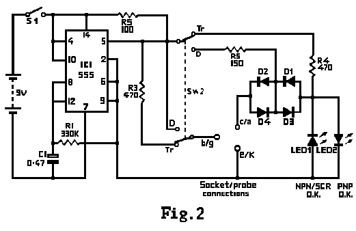
Diodes are added to the circuit to overcome these drawbacks. Fig.1(d) shows the set-up for testing an NPN transistor. The voltage appearing across the collector/emitter terminals is the forward voltage drop across the LED minus that of the two diodes. This is about 0.4V, which is insufficient to cause a diode connected across the terminals to conduct. The reduced voltage available also means that the tester is less affected by in-circuit resistance - in fact it will tolerate values as low as 50 ohms before any dunning of the LEDs occurs. The original circuit before the introduction of the diodes is satisfactory for testing diodes and thyristors with their forward voltage drops of 0.5V to 1V or so. In the final circuit (Fig.2) cancellation of the voltage drops introduced by diodes D1 to D4 is achieved by supplying power to their junction via R5 when the transistor/diode switch is in the diode position.

The diodes could simply be switched out of circuit, of course, but the method adopted allows a suitable resistor value (R5) to be switched in at the same time. This lower value ensures that the same tolerance to in-circuit resistance is retained, though at the cost of increased power consumption.
Thyristors can also be tested with the switch in the diode position. To allow for the fact that these are often insensitive devices, gate bias current is supplied from the positive side of the battery via R2. As the gate is not required to be negative with respect to the cathode, reversal of the supply to it is not necessary.
A 555 dual timer IC is used to provide supply line reversal at about 5Hz. One section of the IC is connected as an astable oscillator with timing components R1 and C1. C1 is charged and discharged from the output at pin 9 via R1. The other section of the IC has its trigger and threshold inputs (pins 2 and 6) connected to pin 9, with the result that its output at pin 5 follows the square wave present at pin 9 but with reversed polarity. When internal voltage drops are taken into account, the net result is a 14V peak-to-peak square wave between pins 5 and 9. This forms the supply for the rest of the circuit.
Components list:
| R1 | 300KW | C1 | 0.47µF (tantalum bead) | D1-D4 | 1N4004 or BA148 | ||||||
| R2 | 100W | LED1 | Green | ||||||||
| R3, R4 | 470W | LED2 | Red | ||||||||
| R5 | 15W | IC1 556 | Green | ||||||||
| All ¼W carbon file 5%. | |||||||||||

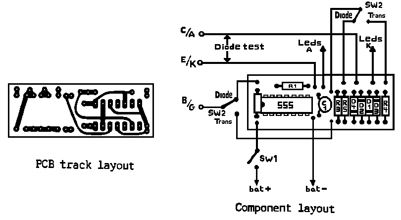
The PCB is small enough to fit into almost any case which will accommodate the battery (PP3 alkaline), but a larger case will allow test sockets to be fitted. (The author used a Vero hand-held case 202-21026G, listed by Maplin as type 401, code LL14Q, with same internal struts cut away to accommodate the battery, and fitted miniature LEDs; the PCB was secured with an adhesive pad. SW1 and SW2 are miniature slide switches). The probes consist of short lengths of plastic covered curtain wire supported in a section of 5A strip connector. Dart points were filed down to a push fit in the ends of the wire, and the assembly was bolted to the bottom of the case through the hole in the connecting strip.
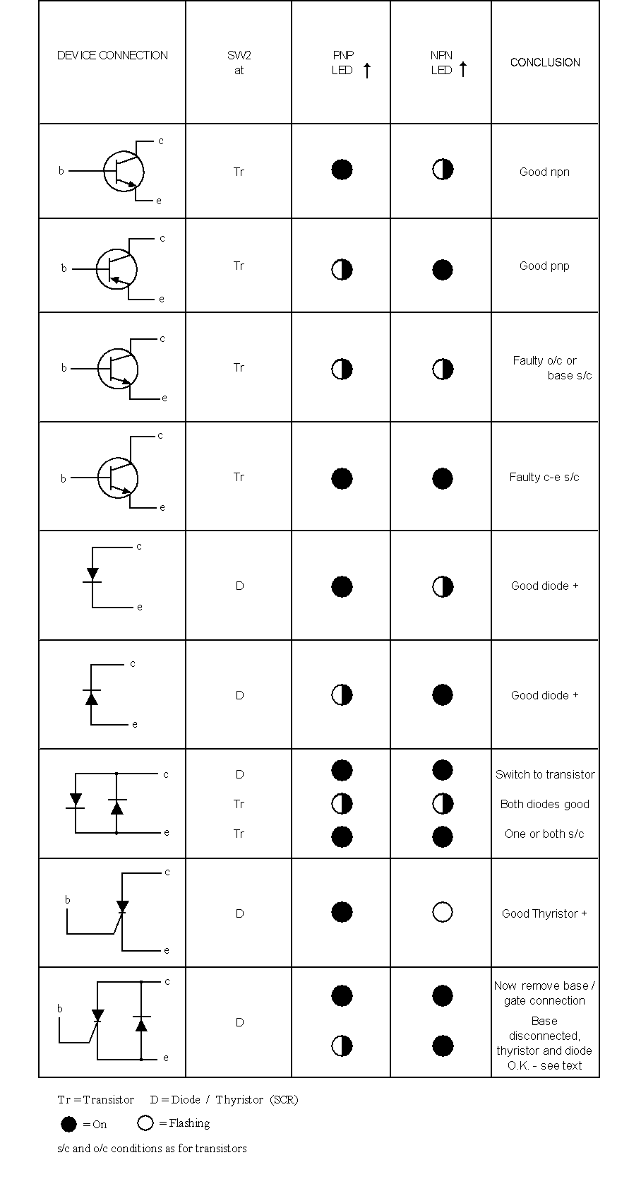
Table 1 lists the main possibilities that may be encountered in using the tester. One LED flashing generally indicates a good device. One of the exceptions is when two diodes are connected back to back. In this case current flows on both half cycles, turning off both LEDs. If this action is in fact due to normal diode current, this will be confirmed by switching to the transistor test position, whereupon both LEDs will turn on again. If they stay off, at least one of the diodes is short-circuit.

If when using the tester one LED extinguishes while the other dims somewhat, this would indicate a suspect device - unless there is an unusual circuit configuration.
Although the tester is basically a go/no-go checker, the majority of semiconductor device faults in practice fall within this category. Its main virtues are that it is quick and easy to use, giving rapid indication of transistor types, diode polarity etc..., while possessing good immunity to in-circuit conditions. More subtle faults caused by semiconductor devices not being quite up to specification, e.g.. low gain and so on, would in any case require a different fault-finding procedure.