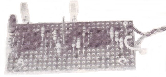
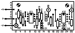
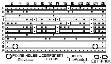
Figure 2. Veroboard layout for CMOS logic probe
Ideally an oscilloscope should be used for testing this type of equipment, but where this is not possible for some reason a logic probe makes an excellent alternative. This simple logic probe is intended for use with CMOS logic circuits, is powered from the circuit under investigation, and has a current consumption of only around 0 to 20mA (depending on the supply voltage and logic state indicated by the probe). The logic state detected by the unit is indicated by a two-LED display: one of the display LEDs IS a multicolour type and the other is an ordinary green type. The following table shows the display obtained from various input signal conditions.
| Input State | D1 | D2 |
|---|---|---|
| Low | Green | Off |
| High | Red | Off |
| Intermediate | Yellow | Off |
| Pulsing fast | Yellow | On |
| Pulsing slowly | Red/Green | Slowly Pulsing |
When the input is pulsing at high speed it is possible that D1 will be red or green instead of yellow, and this simply indicates that the mark-space-ratio of the input signal is far from being one-to-one. D1 will be red if the input is high for the majority of the time, or green if it is predominantly low. If the input is pulsing slowly, unless the pulses are extremely brief, D1 will be seen to switch from red to green and so on in sympathy with the input signal.
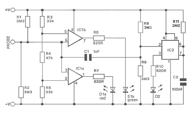
Both sections of IC1 are used as voltage comparators rather than operational amplifiers, and these each have one input connected to a reference voltage, and the other taken to the input of the probe. The unit must indicate a high input state if the input voltage is more than about 70% of the supply voltage, and allow input state if the input is at less than about 30% of the supply potential. R3 to R5 form a potential divider which gives reference voltages of approximately 30% and 70% of the supply voltage.
If the input is low, IC1a's non-inverting input will be at a higher potential than the inverting input so that the output goes high and switches on D1b. IC1b has the opposite input states so that its output goes low and D1a is switched off. This gives a green indication from D1. With the input in the high state IC1a's inverting input is taken to a higher voltage than the non-inverting input, causing the output to go low and switch off D1b. IC1b's non-inverting input will now be at a higher voltage than the inverting input, causing IC1b's output to go high and switch on D1a so that a red indication is obtained from D1.
If the input is between the two logic states the outputs of the two comparators will both assume the high state so that the red and green sections of D1 switch on to produce a yellow display. R1 and R2 bias the input between the two logic levels so that the unit will indicate a fault condition (with D1 in the yellow state) if the input is taken to an open circuit test point.
This section of the circuit does not enable the user to differentiate between a static level between the two logic states and a high frequency pulse signal, since the latter will cause both sections of D1 to switch on in turn and give the impression of a yellow display due to the switching action being too fast to be seen. This is overcome by applying the input signal to the trigger input of a 555 monostable. Normally R8 and R9 hold the input of IC2 above the trigger threshold, but if there IS a pulsing input signal it will be coupled to the input of IC2 by C1 and on negative transistions IC2 will be activated. LED indicator D2 is then switched on for about 0.25 seconds each time IC2 is triggered, but with a high frequency input signal the circuit will be retriggered almost as soon as each output pulse ceases, and D2 will appear to light continuously. C1 blocks steady state inputs so that IC2 is not triggered, except possibly for a single triggering when the input is taken to a new logic state, with a consequent brief flash from D2.
Resistors - ALL Min Res R1,2,8,9 3M3 (Orange Orange Green) 4 off (M3M3) - 13p R3,5 33k (Orange Orange Orange) 2 off (M33K) - 9p R4 47k (Yellow Violet Orange) (M47K) - 9p R6,7,10 820W (Grey Red Brown) 3 off (M820R) - 9p R11 2M2 (Red Red Green) (M2M2) - 13p Colour Code Convertor PC Windows Programme. Very good and easy to us. I recommend it! Capacitors C1 1 nF (103Z) Ceramic 1 (Discontinued) All ceramics are measured in pico farads. So 104 = 10,000 pico farads = 10 nano farads. See Engineering Notations for description of measurements. C2 100n Poly Film (DT98G) - 10p Semiconductors IC1 CA3240E - Use LM393N Voltage Comparator ??? (Discontinued) - Was Ł1.38 IC2 555 Timer - NE555N - replacement for ICM7555 (GH66W) - 37p D1 Common cathode 2 colour LED (Discontinued) D2 [Rectangular] Shape LED R1 Green (YY46A) - 16p Miscellaneous LK1-7 Wire links between circuit tracks. CN1 Gold Croc Clip Red (FS53J) - 52p CN2 Gold Croc Clip Black (FS55K) - 52p One Meter of 2-way Cable for power lead. Logic Probe Tip - Long M3 bolt Small moulded black plastic case (FT31) - 99p 124mm long by 33mm wide by 30mm deep Vero-board, 81 x 14 holes - Stripboard (FL17T) - Ł4.99
All components available from Maplin Electronics on-line (through the Post or from there 40 UK Shops). The Logic Probe project was published in the Maplin Magazine.
![]() Maplin Electronics - postal retailer with shops of 12,000 quality Electronic Components and Items, large stock, own catalogue. P&P Ł2.50, free over Ł35 incl. VAT.
Maplin Electronics - postal retailer with shops of 12,000 quality Electronic Components and Items, large stock, own catalogue. P&P Ł2.50, free over Ł35 incl. VAT.
Robert Penfold