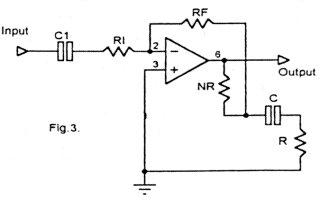
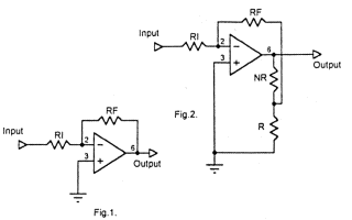
Fig. 1 above shows the classic use of an op-amp as an inverting amplifier. The voltage gain is defined as Rf/R1 and the input impedance is R1. If we want a high input impedance and a high voltage gain, Rf can become very large in value, leading to current offset problems unless an FET input amplifier is used.
Fig. 2 above shows a possible solution to the problem. Here, the ampifier output is attenuated by the two resistors R and NR, the attenuation factor being R + NR/R. The feedback resistor RF is connected to the attenuated output and the voltage gain then becomes (RF(R + NR)/R)R1. This means that the value of the feedback resistor can be reduced by the attenuation factor whilst maintaining the gain.
The technique can be similarly applied to the non-inverting amplifiers and current to voltage convertors in both DC and AC configurations. In the AC configuration, the use of a capacitor makes possible the reduction of DC gain and thus DC offset. Thus:
Where current to voltage convertors are concerned, this can be a useful technique. If, using opto-electronics, we are looking for a fairly small AC signal (optical), in daylight. There are two possible configurations for a photodiode. The first is to use it in reversed bias mode. This mode makes it pretty easy to isolate the AC signal from the DC signal introduced by the ambient illumination but at the expense of very high impedance circuitry (often several megaohms). The second option is to use the photdiode in the photo-amperic (short circuit current) mode. Here, isolation from ambient light is not so easy and a relatively low gain can lead to saturation of the current to voltage convertor due to high ambient light levels. The technique described means that AC conversion gain can be considerably higher than DC conversion gain so that higher gains can be implemented before the amplifier saturates.
I've recently been doing some work on light beam communication using an FM system with a 30KHz "carrier" and decided that I needed to introduce some band pass characteristics to help reduce noise level.
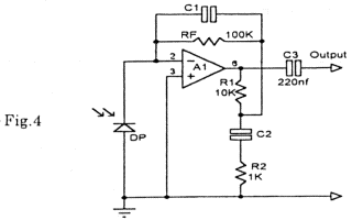
Fig. 4 above, is a photo current to voltage convertor with a difference. It has a much greater conversion factor at AC than at DC and illustrates some of the advantages of negative feedback attenuation.
Where the photodiode current is I, we have a DC conversion such that:
Vout = I(RF + R1)
While the AC conversion factor, (with C1 removed), is:
Vout = I((RF)(R1 + R2 + Xc/(R2 + Xc))
Where Xc is the reactance of the capacitor, C2, at the frequency involved (100nF has a reactance of around 50 Ohms at 30KHz). With C1 in situ and C2 small, the circuit lends itself nicely to also being a band pass filter, as the reactances of both C1 and C2 vary inversely with frequency. C1 gives a measure of "top cut" aided by the bandwidth limitations of the amplifier, whilst C2 gives us "bottom cut".
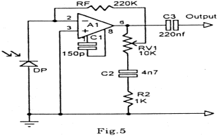
Fig. 5 above, shows R1 replaced by a potentiometer to implement a gain control. With higher values of RF, C1 becomes very small indeed and an alternative strategy is required for top cut. This involves applying a small capacitor to the compensation terminals of the op-amp. To evaluate the characteristics of the circuit, I used it as below:
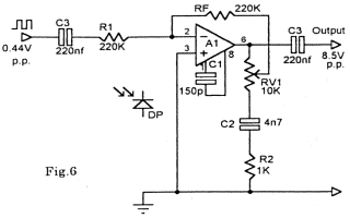
Here, a dummy signal was injected via C3 and R1 to simulate a photodiode current of ±1µA. The results are intresting in that the output is much larger than that predicted by theory! RV1 was fixed at 10K to simplify matters so that the conversion factor should be:
I x 220000 x (10,000 + XC1 + 1000) / (XC1 + 1000) = 1.253 Volts/µA
XC1 was calculated for 30KHz at 1,128 Ohms.
The output then, should be 2.506 V p.p. The measured value was in fact 8.5V p.p. I am baffled by this but I have to accept as evidenced by my eyes.
To convince myself that I wasn't dreaming, I removed the feedback attenuation network (RV1, C2, R2), connecting RF direct to the amplifier output and got precisely what I expected, an output of 0.44 V p.p. and rather distorted at that! Replacing the network brought the signal back at 8.5 V p.p. in the form of a reasonable sine wave.
This clearly demonstrates that the network has an AC attenuation factor of 8.5/0.44 = 19.3 which is ridiculous, especially as I've checked the values of RV1 and R2 with a meter, and even replaced RV1 with a fixed resistor of 10K.
Varying the frequency of the signal shows a roll off on either side of 29KHz, the signal amplitude falling to 8V at 25KHz and 7V at 35KHz. Reducing the value of C1 slightly gave me 7.5V at 35KHz but seemed to introduce some harmonic distortion at the lower end. As the demodulator rejects amplitude modulation I think I'll keep to the original value of 150pF for C1. The harmonic distortion may be largely due to the fact that the original signal does not have an exact 50-50 mark-space ratio. The circuit then produces a more than adequate performance for the purpose envisaged but the enhanced conversion gain has me baffled. Being an empiricist by nature I'm quite happy to accept it as it is but if anyone can come up with an explanation I'd be very pleased to hear it!